Advanced PCB Manufacturing
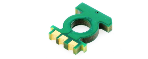
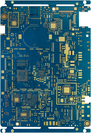
With the rapid development of technology, there is a great demand for advanced PCBs. Now the
advanced PCB has been widely used in high-end and high-precision electronic devices, such as
automotive electronics, complex industrial equipment, complex computing, instrumentation, as well as
communication equipment, etc.
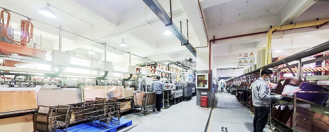
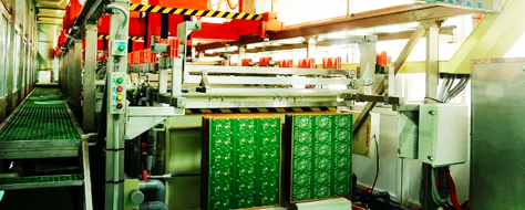
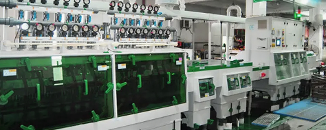
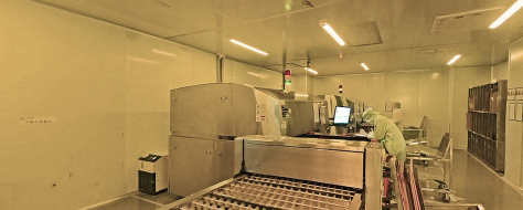
Specialized in the advanced PCB, pcbvertex has fully updated the production
equipment and fabricated your printed circuit board with the advanced technologies.
What’s more, pcbvertex offers mature and high-class quick turn PCB fabrication and
assembly, supported by its three PCB factories covering 17,000 square meters in total.
As printed circuit board technologies increase and electronics continue to get smaller and smaller, you
need to make sure your current circuit board supplier has the appropriate equipment needed for the
specialty processes that are found in more advanced circuit board designs.
Qualified Materials
-
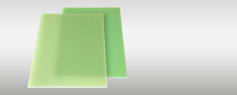
FR-4 Board
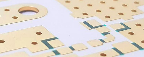
- Aluminum Board
- Copper Base
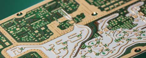
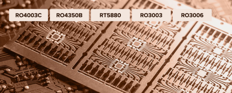
- Rogers
-
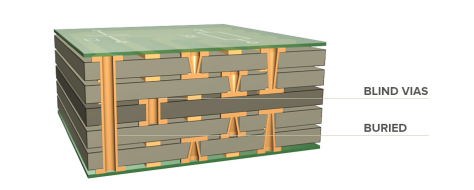
HDI
Buried/
blind vias
-
Iso la:FR402, IS400,FR402, IS400, FR406, FR408, FR408HR,370HR
-
TUC:TU-752, TU-742 Nan Ya
-
Nan Ya:NP-170,NP-180
-
Sheng yi:S1141,S1000H,S1000-2M, S1155G,S1170G,S1600L
-
ITEQ:IT158, IT180,IT140G,IT170G)
-
NELCO:MW4000, MW3000,MW2000,MW1000,N4000-13, N4000-29
-
Immersion gold(ENIG)
- Hard Gold
- ENEPIG
- OSP
-
Immersion silver(Ag)
-
HASL
with lead/
lead free
-
Surface Finish
-
Half-cut/
Castellated
Holes
-
Impedance
control
-
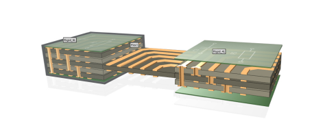
Buried/
blind vias
-
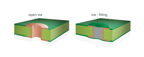
Via filled
with resin
-
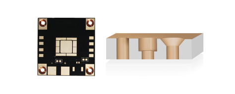
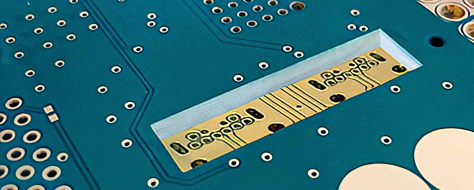
Countersinks/
Counterbores
-
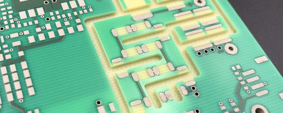
Z-axis milling
-
Custom
Stackup
-
Halogen-Free
-
Additional
Options
pcbvertex PCB Capabilities
|
|
|
-
the Number of layers
|
-
Standard
-
MC PCB
-
HDI interconnect
-
Rogers
|
-
1-14
-
1-2
-
4-14
-
1-14
|
-
Materials
|
-
FR4
-
High TG
-
Halogen Free
-
High Frequency
|
-
Yes
-
TG - 170
-
Yes
-
Yes
|
-
Max PCB size
|
-
|
-
"1layer&2layers: 1200 × 300mm or 600 × 500mm
Multi-layers: 600 × 500mm"
|
-
PCB thickness
|
-
|
-
"1 Layer/2 Layers: 0.2~2.4mm
-
4 Layers: 0.4~2.4mm
-
6 Layers: 0.8~2.4mm
-
8 Layers: 1.0~2.4mm
-
10 Layers: 1.2~2.4mm
-
Note: Customized PCB thickness and Layer stack up are acceptable."
|
-
Min width
|
-
|
-
3mils
|
-
Min space
|
-
|
-
3mils
|
-
Outer max cooper
|
-
|
-
"1oz/2oz/3oz
(35μm/70μm/105μm)
Note:
2oz
PCB thickness≥1.2mm,
Via size≥0.25mm,
Min Track/Spacing≥0.15mm
3oz
PCB thickness≥2.0mm,
Via size≥0.3mm,
Min Track/Spacing≥0.2mm"
|
-
Inner max copper
|
-
|
-
"1oz/1.5oz (35μm/50μm)"
|
-
Min CNC finished aperture
|
-
0.15mm
|
-
Yes
|
-
Min Laser finished aperture
|
-
0.1mm
|
-
Yes
|
-
Max aspect ratio
|
-
|
-
12 : 1
|
-
Solder mask color
|
-
Green/Red/Yellow/Blue/White/Purple/Black/
Matte black/Matte green/None
|
-
Yes
|
-
Impedance control tolerance
|
-
|
-
Yes
|
-
Min annular ring
|
-
|
-
3mil
|
-
Panelization
|
-
"V-scoring, Tab-routing,
Tab-routing with Perforation (Stamp Holes)"
|
-
Yes
|

.png)
.png)
